- Source or sink:
––2,000W of pulsed power (±40V, ±50A)
––200W of DC power (±10V@±20A, ±20V@±10A, ±40V@±5A) - Easily connect two units (in series or parallel) to create solutions up to ±100A or ±80V
- 1pA resolution enables precise measurement of very low leakage currents
- 1μs per point (1MHz), 18-bit sampling, accurately characterizes transient behavior
- 1% to 100% pulse duty cycle for pulse width modulated (PWM) drive schemes and devicespecific drive stimulus
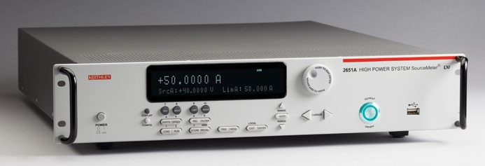
- Combines a precision power supply, current source, DMM, arbitrary waveform generator, V or I pulse generator with measurement, electronic load, and trigger controller—all in one instrument
- Includes TSP® Express I-V characterization software, LabVIEW® driver, and Keithley’s
Test Script Builder software development environment
APPLICATIONS
- Power semiconductor, HBL ED, and optical device characterization and testing
- Solar cell characterization and testing
- Characterization of GaN, SiC, and other compound materials and devices
- Semiconductor junction temperature characterization
- High speed, high precision digitization
- Electromigration studies
- High current, high power device testing
| pecification Conditions | |||||||
| This document contains specifications and supplemental information for the Model 2651A High Power System SourceMeter SMU instrument. Specifications are the standards against which the Model 2651A is tested. Upon leaving the factory, the Model 2651A meets these specifications. Supplemental and typical values are non-warranted, apply at 23°C, and are provided solely as useful information. Source and measurement accuracies are specified at the Model 2651A terminals under these conditions: • 23° ±5°C, <70 percent relative humidity • After two-hour warm-up • Speed normal (1 NPLC) • A/D autozero enabled • Remote sense operation or properly zeroed local operation • Calibration period: One year Accuracy specifications are applicable for both normal and high-capacitance modes. |
|||||||
| VOL TAGE ACCURA CY SPECIFICATIONS 1, 2 | |||||||
| SOURCE | MEASURE | ||||||
| range | Programming resolution | accuracy ±(% reading + volts) | Noise (Vpp) (typical) 0.1 Hz to 10 Hz | Default Display resolution | Integrating aDC accuracy 3 ±(% reading + volts) | High-speed aDC accuracy 4 ±(% reading + volts) | |
| 100 .000 mV | 5 µV | 0 .02% + 500 µV | 100 µV | 1 µV | 0 .02% + 300 µV | 0 .05% + 600 µV | |
| 1 .00000 V | 50 µV | 0 .02% + 500 µV | 500 µV | 10 µV | 0 .02% + 300 µV | 0 .05% + 600 µV | |
| 10 .0000 V | 500 µV | 0 .02% + 5 mV | 1 mV | 100 µV | 0 .02% + 3 mV | 0 .05% + 8 mV | |
| 20 .0000 V | 500 µV | 0 .02% + 5 mV | 1 mV | 100 µV | 0 .02% + 5 mV | 0 .05% + 8 mV | |
| 40 .0000 V | 500 µV | 0 .02% + 12 mV | 2 mV | 100 µV | 0 .02% + 12 mV | 0 .05% + 15 mV | |
| CURR ENT ACCURA CY SPECIFICATIONS 5 | |||||||
| SOURCE | MEASURE | ||||||
| range | Programming resolution | accuracy ±(% reading + volts) | Noise (Vpp) (typical) 0.1 Hz to 10 Hz | Default Display resolution | Integrating aDC accuracy 3 ±(% reading + volts) | High-speed aDC accuracy 4 ±(% reading + volts) | |
| 100 .000 nA | 2 pA | 0 .1 % + 500 pA | 50 pA | 1 pA | 0 .08% + 500 pA | 0 .08% + 800 pA | |
| 10 .0000 µA | 200 pA | 0 .1 % + 10 nA | 500 pA | 100 pA | 0 .08% + 8 nA | 0 .08% + 10 nA | |
| 1 .00000 mA | 20 nA | 0 .03% + 300 nA | 10 nA | 10 nA | 0 .02% + 200 nA | 0 .05% + 500 nA | |
| 100 .000 mA | 2 µA | 0 .03% + 30 µA | 1 µA | 1 µA | 0 .02% + 20 µA | 0 .05% + 50 µA | |
| 5 .00000 A | 200 µA | 0 .08% + 3 .5 mA | 300 µA | 10 µA | 0 .05% + 3 mA | 0 .05% + 5 mA | |
| 20 .0000 A | 500 µA | 0 .15% + 8 mA | 500 µA | 100 µA | 0 .08% + 8 mA | 0 .08% + 15 mA | |
| NOTES 1. Add 50μV to source accuracy specifications per volt of HI lead drop. 2. For temperatures 0° to 18°C and 28° to 50°C, accuracy is degraded by ±(0.15 × accuracy specification)/°C. High-capacitance mode accuracy is applicable at 23° ±5°C only. 3. Derate accuracy specification for NPLC setting <1 by increasing error term. Add appropriate typical percent of range term for resistive loads using the table below. |
|||||||
| NPlC setting | 100mV range | 1V to 40V ranges | 100na range | 1µa to 100ma ranges | 1a to 20a ranges | ||
| 0 .1 | 0 .01% | 0 .01% | 0 .01% | 0 .01% | 0 .01% | ||
| 0 .01 | 0 .08% | 0 .07% | 0 .1 % | 0 .05% | 0 .1 % | ||
| 0 .001 | 0 .8 % | 0 .6 % | 0,01 | 0 .5 % | 1 .8 % | ||
| 4. 18-bit ADC. Average of 1000 samples taken at 1μs intervals. 5. At temperatures 0° to 18°C and 28° to 50°C; 100nA to 10μA accuracy is degraded by ±(0.35 × accuracy specification)/°C. 100μA to 50A accuracy is degraded by ±(0.15 × accuracy specification)/°C. High-capacitance mode accuracy is applicable at 23° ±5°C only. 6. 50A range accessible only in pulse mode. 7. 50A range accuracy measurements are taken at 0.008 NPLC. 8. Average of 100 samples taken at 1μs intervals |
|||||||
| DC POWER SPECIFICATIONS | |||||||
| Maximum output power : | 202W maximum. | ||||||
| Source /Sink Limits 1: | Voltage: ±10.1V at ±20.0A, ±20.2V at ±10.0A, ±40.4V at ±5.0A 2. Four-quadrant source or sink operation. Current: ±5.05A at ±40V 2, ±10.1A at ±20V, ±20.2A at ±10V Four-quadrant source or sink operation. |
||||||
| CAUTION: Carefully consider and configure the appropriate output-off state and source and compliance levels before connecting the Model 2651A to a device that can deliver energy. Failure to consider the output-off state and source and compliance levels may result in damage to the instrument or to the device under test. |
|||||||
| Pulse SPECIFICATIONS | 100μs. Note: Minimum pulse width for settled source at a given I/V output and load can be longer than 100μs. |
||||||
| Pulse width programming resolution : | 1μs. | ||||||
| Pulse width programming accurac y 3: | ±5μs. | ||||||
| Pulse width jitter | 2μs (typical). | ||||||
| Pulse Rise Time (typical ): | |||||||
| Current Range | Rload | Rise Time (typical) | |||||
| 50 A | 0 .05 Ω | 26 µs | |||||
| 50 A | 0 .2 Ω | 57 µs | |||||
| 50 A | 0 .4 Ω | 85 µs | |||||
| 20 A | 0 .5 Ω | 95 µs | |||||
| 50 A | 0 .8 Ω | 130 µs | |||||
| 20 A | 1 Ω | 180 µs | |||||
| 10 A | 2 Ω | 330 µs | |||||
| 5 A | 8 .2 Ω | 400 µs | |||||
| region | Region Maximums |
Maximum Pulse Width 3 |
Maximum Duty Cycle 4 |
||||
| 1 | 5 A at 40 V | DC, no limit | 100% | ||||
| 1 | 10 A at 20 V | DC, no limit | 100% | ||||
| 1 | 20 A at 10 V | DC, no limit | 100% | ||||
| 2 | 30 A at 10 V | 1 ms | 50% | ||||
| 3 | 20 A at 20 V | 1 .5 ms | 40% | ||||
| 4 | 10 A at 40 V | 1 .5 ms | 40% | ||||
| 5 | 50 A at 10 V | 1 ms | 35 | ||||
| 6 | 50 A at 20 V | 330 µs | 10% | ||||
| 7 | 50 A at 40 V | 300 µs | 1% | ||||
| NOTES 1. Full power source operation regardless of load to 30°C ambient. Above 30°C or power sink operation, refer to “Operating Boundaries” in the Model 2651A Reference manual for additional power derating information. 2. Quadrants 2 and 4 power envelope is trimmed at 36V and 4.5A. 3. Times measured from the start of pulse to the start off-time; see figure below. 4. Thermally limited in sink mode (quadrants 2 and 4) and ambient temperatures above 30°C. See power equations in the Model 2651A Reference Manual for more information. |
|||||||
| ADDITIONAL SOUR CE SPECIFICATIONS | |||||||
| Noise (10Hz to 20MHz): | <100mV peak-peak (typical), <30mV RMS (typical), 10V range with a 20A limit. |
||||||
| Overshoot : | Voltage: <±(0.1% + 10mV) (typical). Step size = 10% to 90% of range, resistive load, maximum current limit/compliance. Current: <±(0.1% + 10mV) (typical). Step Size = 10% to 90% of range, resistive load. See Current Source Output Settling Time specifications for additional test conditions. |
||||||
| Range change overshoot : | Voltage: <300mV + 0.1% of larger range (for <20V ranges) (typical). <400mV + 0.1% of larger range (for ≥20V ranges) (typical). Overshoot into a 100kW load, 20MHz bandwidth. Current: <5% of larger range + 360mV/Rload (for >10μA ranges) (typical). Iout × Rload = 1V. |
||||||
| Voltage source output settling time : | Time required to reach within 0.1% of final value after source level command is processed on a fixed range. 1 |
||||||
| Range | Settling Time (typical) | ||||||
| 1 V | < 70 µs | ||||||
| 10 V | <160 µs | ||||||
| 20 V | <190 µs | ||||||
| 40 V | <175 µs | ||||||
| Current source output settling time : Time required to reach within 0.1% of final value after source level command is processed on a fixed range. Values below for Iout × Rload. |
|||||||
| Transient response time : | 10V and 20V Ranges: <70μs for the output to recover to within 0.1% for a 10% to 90% step change in load. 40V Range: <110μs for the output to recover to within 0.1% for a 10% to 90% step change in load. |
||||||
| Guard offset voltage : | <4mV, current <10mA. | ||||||
| Remote sense operating range 2: | Maximum Voltage between HI and SENSE HI: 3V. Maximum Voltage between LO and SENSE LO: 3V. |
||||||
| Maximum impedance per source lead : | Maximum impedance limited by 3V drop by remote sense operating range. Maximum resistance = 3V/source current value (amperes) (maximum of 1W per source lead). 3V = L di/dt. |
||||||
| Voltage output headroom : | 5A Range: Maximum output voltage = 48.5V – (Total voltage drop across source leads). 10A Range: Maximum output voltage = 24.5V – (Total voltage drop across source leads). 20A Range: Maximum output voltage = 15.9V – (Total voltage drop across source leads). |
||||||
| Overtemperature protection : | Internally sensed temperature overload puts unit in standby mode. |
||||||
| Limit /compliance | Bipolar limit (compliance) set with single value. Voltage 3: Minimum value is 10mV; accuracy is the same as voltage source. Current 4: Minimum value is 10nA; accuracy is the same as current source. |
||||||
| NOTES 1. With measure and compliance set to the maximum current for the specified voltage range. 2. Add 50μV to source accuracy specifications per volt of HI lead drop. 3. For sink mode operation (quadrants II and IV), add 0.6% of limit range to the corresponding voltage source accuracy specifications. For 100mV range add an additional 60mV of uncertainty. Specifications apply with sink mode enabled. 4. For sink mode operation (quadrants II and IV), add 0.6% of limit range to the corresponding current limit accuracy specifications. Specifications apply with sink mode enabled. |
|||||||
| Measurement Speed Speci fic ati ons 1, 2 | |||||||
| Maxim um SWEEP OPERA TION RA TES (operations per second) FOR 60Hz (50Hz): | |||||||
| a/D Converter speed | Trigger origin | Measure To Memory using user scripts | Measure To GPIb using user scripts | source Measure To Memory using user scripts | source Measure To GPIb using user scripts | source Measure To Memory using sweep aPI | source Measure To GPIb using sweep aPI |
| 0 .001 NPLC | Internal | 20000 (20000) | 9800 (9800) | 7000 (7000) | 6200 (6200) | 12000 (12000) | 5900 (5900) |
| 0 .001 NPLC | Digital I/O | 8100 (8100) | 7100 (7100) | 5500 (5500) | 5100 (5100) | 11200 (11200) | 5700 (5700) |
| 0 .01 NPLC | Internal | 4900 (4000) | 3900 (3400) | 3400 (3000) | 3200 (2900) | 4200 (3700) | 4000 (3500) |
| 0 .01 NPLC | Digital I/O | 3500 (3100) | 3400 (3000) | 3000 (2700) | 2900 (2600) | 4150 (3650) | 3800 (3400) |
| 0 .1 NPLC | Internal | 580 (480) | 560 (470) | 550 (465) | 550 (460) | 560 (470) | 545 (460) |
| 0 .1 NPLC | Digital I/O | 550 (460) | 550 (460) | 540 (450) | 540 (450) | 560 (470) | 545 (460) |
| 1 .0 NPLC | Internal | 59 (49) | 59 (49) | 59 (49) | 59 (49) | 59 (49) | 59 (49) |
| 1 .0 NPLC | Digital I/O | 58 (48) | 58 (49) | 59 (49) | 59 (49) | 59 (49) | 59 (49) |
| HS ADC | Internal | 38500 (38500) | 18000 (18000) | 10000 (10000) | 9500 (9500) | 14300 (14300) | 6300 (6300) |
| HS ADC | Digital I/O | 12500 (12500) | 11500 (11500) | 7500 (7500) | 7000 (7000) | 13200 (13200) | 6000 (6000) |
| High Speed ADC Burst MEASUR EMENT RA TES 3 | |||||||
| Burst Length (readings) | Readings per Second | Bursts per Second | |||||
| 100 | 1,000,000 | 400 | |||||
| 500 | 1,000,000 | 80 | |||||
| 1000 | 1,000,000 | 40 | |||||
| 2500 | 1,000,000 | 16 | |||||
| 5000 | 1,000,000 | 8 | |||||
| Maxim um SINGLE MEASUR EMENT RA TES (operations per second) FOR 60Hz (50Hz) | |||||||
| source | Measure | ||||||
| a/D Converter | Trigger | Measure | Measure | Pass/fail | |||
| speed | origin | To GPIb | To GPIb | To GPIb | |||
| 0 .001 NPLC | Internal | 1900 (1800) | 1400 (1400) | 1400 (1400) | |||
| 0 .01 NPLC | Internal | 1450 (1400) | 1200 (1100) | 1100 (1100) | |||
| 0 .1 NPLC | Internal | 450 (390) | 425 (370) | 425 (375) | |||
| 1 .0 NPLC | Internal | 58 (48) | 57 (48) | 57 (48) | |||
| Maximum Measurement RANGE CHANGE RATE: | >4000 per second for >10μA (typical). | ||||||
| Maximum SOURCE Range CHANGE RATE: | >325 per second for >10μA, typical. When changing to or from a range ≥1A, maximum rate is >250 per second, typical. |
||||||
| COMMAND PROCESSING TIME: | Maximum time required for the output to begin to change following the receipt of the smua.source.levelv or smua.source.leveli command. <1ms typical. |
||||||
| NOTES 1. Tests performed with a Model 2651A on channel A using the following equipment: Computer hardware (Intel® Pentium® 4 2.4GHz, 2GB RAM, National Instruments™ PCI-GPIB). Driver (NI-488.2 Version 2.2 PCI-GPIB). Software (Microsoft® Windows® XP, Microsoft Visual Studio® 2010, VISA™ version 4.1). 2. Exclude current measurement ranges less than 1mA. 3. smua.measure.adc has to be enabled and the smua.measure.count set to the burst length. |
|||||||
| TRIGGERING AND SYNCHRO NIZATION SPECIFICATIONS | |||||||
| Triggering : | Trigger In to Trigger Out: 0.5μs (typical). Trigger In to Source Change 1: 10μs (typical). Trigger Timer Accuracy: ±2μs (typical). Source Change 1 After LXI Trigger: 280μs (typical). |
||||||
| Synchroni zation : | Single-Node Synchronized Source Change 1: <0.5μs (typical). Multi-Node Synchronized Source Change 1: <0.5μs (typical). |
||||||
| NOTES 1. Fixed source range with no polarity change. |
|||||||
| GENERAL | |||||||
| Connector: | 25-pin female D. | ||||||
| Input/Output Pins: | 14 open drain I/O bits. | ||||||
| Absolute Maximum Input Voltage: | 5.25V. | ||||||
| Absolute Minimum Input Voltage: | –0.25V. | ||||||
| Maximum Logic Low Input Voltage: | 0.7V, +850μA max. | ||||||
| Minimum Logic High Input Voltage: | 2.1V, +570μA. | ||||||
| Maximum Source Current (flowing out of digital I/O bit): | +960μA. | ||||||
| Maximum Sink Current At Maximum Logic Low Voltage (0.7): | –5.0mA. | ||||||
| Absolute Maximum Sink Current (flowing into digital I/O pin): | –11mA. | ||||||
| 5V Power Supply Pin: | Limited to 250mA, solid-state fuse protected. | ||||||
| Output Enable Pin: | Active high input pulled down internally to ground with a 10kW resistor; when the output enable input function has been activated, the Model 2651A channel will not turn on unless the output enable pin is driven to >2.1V (nominal current = 2.1V/10kW = 210μA). |
||||||
| IEEE-488: | IEEE-488.1 compliant. Supports IEEE-488.2 common commands and status model topology. |
||||||
| RS-232: | Baud rates from 300bps to 115200bps. Programmable number of data bits, parity type, and flow control (RTS/CTS hardware or none). When not programmed as the active host interface, the Model 2651A can use the RS-232 interface to control other instrumentation. |
||||||
| Ethernet : | RJ-45 connector, LXI, 10/100BT, Auto MDIX. | ||||||
| LXI compliance : | LXI Class C 1.2. Total Output Trigger Response Time: 245μs minimum, 280μs (typical), (not specified) maximum. Receive Lan[0-7] Event Delay: Unknown. Generate Lan[0-7] Event Delay: Unknown. |
||||||
| Expansion interface : | The TSP-Link Technology expansion interface allows TSP-enabled instruments to trigger and communicate with each other. Cable Type: Category 5e or higher LAN crossover cable. 3 meters maximum between each TSP-enabled instrument. |
||||||
| USB: | USB 2.0 host controller. | ||||||
| Power suppl y: | 100V to 250V AC, 50Hz to 60Hz (autosensing), 550VA maximum. | ||||||
| Cooling : | Forced air; side and top intake and rear exhaust. | ||||||
| Warrant y: | 1 year. | ||||||
| EMC: | Conforms to European Union EMC Directive. | ||||||
| Safet y: | UL listed to UL61010-1:2004. Conforms to European Union Low Voltage Directive. | ||||||
| Dimensions : | 89mm high × 435mm wide × 549mm deep (3.5 in. × 17.1 in. × 21.6 in.). | ||||||
| Bench Configuration (with handle and feet): | 104mm high × 483mm wide × 620mm deep (4.1 in. × 19 in. × 24.4 in.). |
||||||
| Weight : | 9.98kg (22 lbs). | ||||||
| Environment : | For indoor use only. | ||||||
| Altitude : | Maximum 2000 meters above sea level. | ||||||
| Operatin g: | 0° to 50°C, 70% relative humidity up to 35°C. Derate 3% relative humidity/°C, 35° to 50°C. |
||||||
| Storage : | –25° to 65°C. | ||||||